Profile overview
Who is Nobukazu Teranishi?
Nobukazu Teranishi is an inventor associated with Japan. Their documented work in imaging & audio includes Pinned photodiode image sensor, the contribution at the center of this evidence-backed profile.
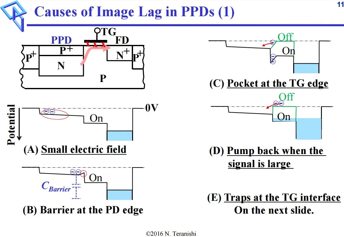
Nobukazu Teranishi invented the pinned photodiode at NEC in 1980. By suppressing image lag and noise while allowing smaller pixels, the physical sensor structure raised image quality and resolution and became a core element of the CCD and CMOS image sensors used in cameras, phones, vehicles, medical instruments and scientific imaging.
What did Nobukazu Teranishi invent?
Invented the pinned photodiode structure used inside modern solid-state image sensors.
What did Nobukazu Teranishi accomplish?
The pinned photodiode became the light-capturing structure in most modern image sensors, quietly sitting behind billions of digital pictures.
What is known about Nobukazu Teranishi today?
The International Image Sensor Society's 2025 workshop program lists Teranishi as an author on current image-sensor research from Shizuoka University's Research Institute of Electronics.


)